- 您现在的位置:买卖IC网 > Sheet目录342 > MCBSTM32EXL (Keil)BOARD EVALUATION FOR STM32F103ZE
�� �
�
�RM0008�
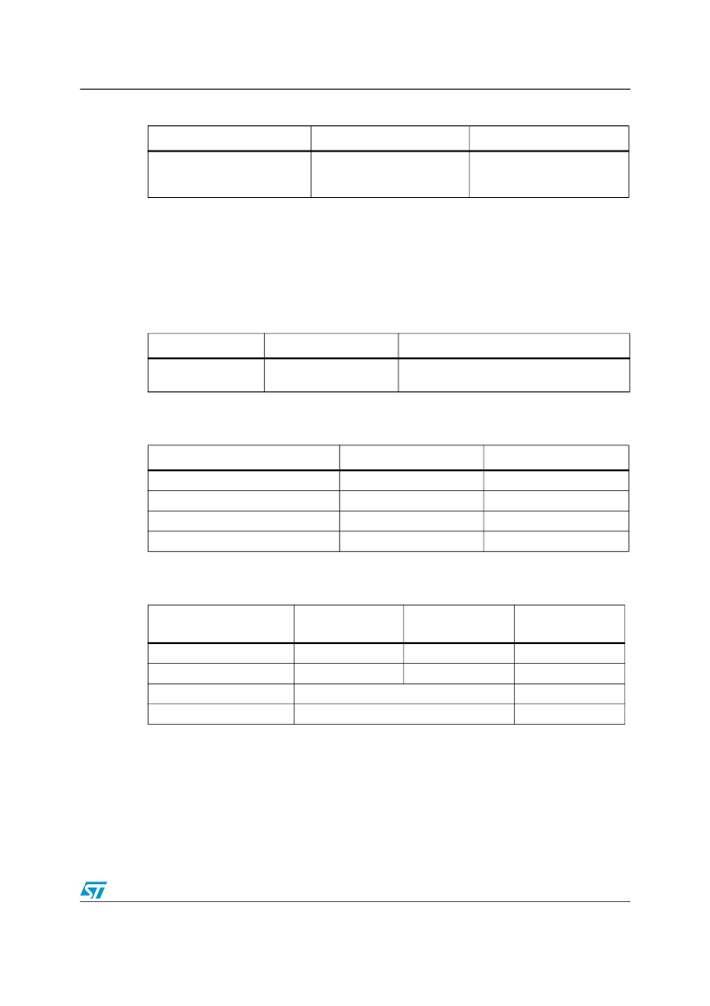
�Table� 37.�
�General-purpose� and� alternate-function� I/Os� (GPIOs� and� AFIOs)�
�ADC2� external� trigger� regular� conversion� alternate� function� remapping� (1)�
�Alternate� function�
�ADC2� external� trigger� regular�
�conversion�
�ADC2_ETRGREG_REG� =� 0�
�ADC2� external� trigger� regular�
�conversion� is� connected� to�
�EXTI11�
�ADC2_ETRGREG_REG� =� 1�
�ADC2� external� trigger� regular�
�conversion� is� connected� to�
�TIM8_TRGO�
�1.� Remap� available� only� for� high-density� devices.�
�8.3.7�
�Timer� alternate� function� remapping�
�Timer� 4� channels� 1� to� 4� can� be� remapped� from� Port� B� to� Port� D.� Other� timer� remapping�
���Table� 38.�
�TIM5� alternate� function� remapping� (1)�
�Alternate� function�
�TIM5_CH4�
�TIM5CH4_IREMAP� =� 0�
�TIM5� Channel4� is�
�connected� to� PA3�
�TIM5CH4_IREMAP� =� 1�
�LSI� internal� clock� is� connected� to� TIM5_CH4�
�input� for� calibration� purpose.�
�1.� Remap� available� only� for� high-density� and� connectivity� line� devices.�
�Table� 39.�
�TIM4� alternate� function� remapping�
�Alternate� function�
�TIM4_CH1�
�TIM4_CH2�
�TIM4_CH3�
�TIM4_CH4�
�TIM4_REMAP� =� 0�
�PB6�
�PB7�
�PB8�
�PB9�
�TIM4_REMAP� =� 1� (1)�
�PD12�
�PD13�
�PD14�
�PD15�
�1.� Remap� available� only� for� 100-pin� and� for� 144-pin� package.�
�Table� 40.�
�TIM3� alternate� function� remapping�
�Alternate� function�
�TIM3_REMAP[1:0]� =� TIM3_REMAP[1:0]� =� TIM3_REMAP[1:0]� =�
�“00”� (no� remap)� “10”� (partial� remap)� “11”� (full� remap)� (1)�
�TIM3_CH1�
�TIM3_CH2�
�TIM3_CH3�
�TIM3_CH4�
�PA6�
�PA7�
�PB0�
�PB1�
�PB4�
�PB5�
�PC6�
�PC7�
�PC8�
�PC9�
�1.� Remap� available� only� for� 64-pin,� 100-pin� and� 144-pin� packages.�
�Doc� ID� 13902� Rev� 9�
�155/995�
�发布紧急采购,3分钟左右您将得到回复。
相关PDF资料
MCBTMPM330
BOARD EVAL TOSHIBA TMPM330 SER
MCIMX25WPDKJ
KIT DEVELOPMENT WINCE IMX25
MCIMX53-START-R
KIT DEVELOPMENT I.MX53
MCM69C432TQ20
IC CAM 1MB 50MHZ 100LQFP
MCP1401T-E/OT
IC MOSFET DRVR INV 500MA SOT23-5
MCP1403T-E/MF
IC MOSFET DRIVER 4.5A DUAL 8DFN
MCP1406-E/SN
IC MOSFET DVR 6A 8SOIC
MCP14628T-E/MF
IC MOSFET DVR 2A SYNC BUCK 8-DFN
相关代理商/技术参数
MCBSTM32EXLU
功能描述:开发板和工具包 - ARM EVAL BOARD + ULINK2 FOR STM32F103ZG
RoHS:否 制造商:Arduino 产品:Development Boards 工具用于评估:ATSAM3X8EA-AU 核心:ARM Cortex M3 接口类型:DAC, ICSP, JTAG, UART, USB 工作电源电压:3.3 V
MCBSTM32EXLU-ED
制造商:ARM Ltd 功能描述:KEIL STM STM32EXL EVAL BOARD
MCBSTM32EXLUME
功能描述:开发板和工具包 - ARM EVAL BOARD + ULINKME FOR STM32F103ZG
RoHS:否 制造商:Arduino 产品:Development Boards 工具用于评估:ATSAM3X8EA-AU 核心:ARM Cortex M3 接口类型:DAC, ICSP, JTAG, UART, USB 工作电源电压:3.3 V
MCBSTM32F200
功能描述:开发板和工具包 - ARM EVAL BOARD FOR STM STM32F207IG
RoHS:否 制造商:Arduino 产品:Development Boards 工具用于评估:ATSAM3X8EA-AU 核心:ARM Cortex M3 接口类型:DAC, ICSP, JTAG, UART, USB 工作电源电压:3.3 V
MCBSTM32F200U
功能描述:开发板和工具包 - ARM EVAL BOARD FOR STM STM32F207IG + ULINK2
RoHS:否 制造商:Arduino 产品:Development Boards 工具用于评估:ATSAM3X8EA-AU 核心:ARM Cortex M3 接口类型:DAC, ICSP, JTAG, UART, USB 工作电源电压:3.3 V
MCBSTM32F200UME
功能描述:开发板和工具包 - ARM EVAL BOARD FOR STM STM32F207IG ULINK-ME
RoHS:否 制造商:Arduino 产品:Development Boards 工具用于评估:ATSAM3X8EA-AU 核心:ARM Cortex M3 接口类型:DAC, ICSP, JTAG, UART, USB 工作电源电压:3.3 V
MCBSTM32F200UME-ED
制造商:ARM Ltd 功能描述:KEIL STM32F207IG EVAL BOARD
MCBSTM32F400
功能描述:开发板和工具包 - ARM EVAL BOARD FOR STM STM32F407IG
RoHS:否 制造商:Arduino 产品:Development Boards 工具用于评估:ATSAM3X8EA-AU 核心:ARM Cortex M3 接口类型:DAC, ICSP, JTAG, UART, USB 工作电源电压:3.3 V